16 years one-stop China custom CNC machining parts factory

Hey there I’m VMT Sam!
With 25 years of CNC machining experience we are committed to helping clients overcome 10000 complex part-processing challenges all to contribute to a better life through intelligent manufacturing. Contact us now
 61 |
Published by VMT at Jul 13 2026 | Reading Time:About 4 minutes
61 |
Published by VMT at Jul 13 2026 | Reading Time:About 4 minutes


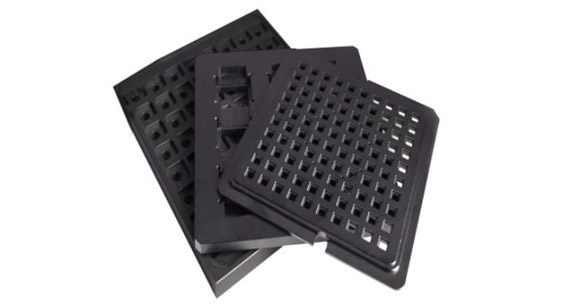
For semiconductor manufacturing, IC testing, and the operation of high-precision electronic equipment,ESD control is vital for system stability. While these products rely on anti-static engineering plastics, traditional options (filled with carbon fiber, carbon black, or carbon nanotubes) risk dielectric breakdown and electrical leakage.
This is where Semitron® ESd 520HR comes in. Based on PAI resin, this benchmark material for high-end electrostatic dissipation offers excellent dielectric breakdown resistance and voltage stability. It also combines PAI’s inherent thermal stability (up to 260°C) with a low coefficient of thermal expansion. However, it has limitations: high water absorption and chemical sensitivity.
This article provides a comprehensive engineering guide to Semitron 520HR, covering its core properties, typical precision part applications, cost , and error-proofing strategies in CNC machining parts design. Finally, we’ll share a factory case study on solving micro-cracking and out-of-tolerance issues in Semitron 520HR parts.
What is Semitron ESd 520HR?
Semitron® ESd 520HR is a high-end electrostatic dissipative (ESD) specialty engineering plastic based on polyamide-imide (PAI) resin. It was specifically developed for semiconductor manufacturing, integrated circuit (IC) testing, and advanced electronic equipment fields, aiming to solve the industry problem where traditional anti-static plastics (such as carbon fiber reinforced, carbon black, or carbon nanotube filled materials) easily fail under high electric field working conditions.
Through modification processes, Semitron ESd 520HR maintains a stable surface resistivity of 10¹⁰ to 10¹² Ohms/sq while providing excellent resistance to high-voltage breakdown (maintaining stable electrostatic dissipation performance even within a high voltage range of 100V to 1000V). Furthermore, it inherits the ultra-high mechanical rigidity and thermal tolerance of its PAI base resin, making it a premium material choice for semiconductor back-end precision test fixtures and front-end wafer handling components.
Semitron ESd 520HR Comprehensive Property Table
Below is the core performance indicator data for Semitron ESd 520HR based on ASTM and ISO standard testing, provided for your engineering reference and data comparison:
| Property |
Test Standard |
Typical Value |
Performance / Behavior |
| Density / Specific Gravity | ASTM D792 | 1.58 g/cm³ | Dense material texture, providing a foundation for a high-rigidity structure. |
| 24-Hour Water Absorption | ASTM D570 | 0.60 % | Significant tendency to absorb water; processing and storage require temperature and humidity control. |
| Saturation Water Absorption | ASTM D570 | 4.6 % | Long-term exposure to high-humidity environments will cause minor dimensional tolerance drift. |
| Tensile Strength | ASTM D638 | 82.7 MPa | Demonstrates high-strength load-bearing capacity; structural components do not easily fracture. |
| Elongation at Break | ASTM D638 | 3.0 % | Low elongation, indicating a tendency toward material brittleness. |
| Tensile Modulus of Elasticity | ASTM D638 | 5520 MPa | Excellent rigidity; minimal deformation when subjected to tensile stress. |
| Flexural Strength | ASTM D790 | 138 MPa | Strong resistance to bending; suitable for use as high-load bearing plates. |
| Flexural Modulus of Elasticity | ASTM D790 | 5860 MPa | Extremely high resistance to flexural deformation, ensuring the flatness of fixtures. |
| Compressive Strength (10% Deformation) | ASTM D695 | 207 MPa | Excellent compression resistance; suitable for high-density test sockets and pin plates. |
| Shear Strength | ASTM D732 | 86.9 MPa | Demonstrates good performance against mechanical shear stress. |
| Rockwell Hardness | ASTM D785 | M 108 | High surface hardness, wear-resistant, and not easily scratched. |
| Izod Notched Impact Strength | ASTM D256 | 0.427 J/cm | Sensitive to stress concentration; sharp corners must be avoided in part design. |
| Coefficient of Linear Thermal Expansion (CLTE) | ASTM E831 | 35 x 10⁻⁶ m/(m·K) | Extremely low expansion coefficient; maintains micron-level tolerances during thermal cycling. |
| Thermal Conductivity | ASTM F433 | 0.357 W/(m·K) | Poor thermal conductivity; local cutting heat accumulation must be strictly prevented during CNC machining. |
| Continuous Service Temperature | Long-term | 250 °C to 260 °C | High thermal stability; can work long-term under high-temperature burn-in/aging test conditions. |
| Heat Deflection Temperature (@264 psi) | ASTM D648 | 271 °C | Retains structural rigidity under the dual effects of high load and high temperature. |
| Glass Transition Temperature (Tg) | ASTM D3418 | 275 °C to 280 °C | The molecular segments of the base material remain highly stable at high temperatures. |
| Surface Resistivity | ESD STM 11.11 | 10¹⁰ to 10¹² Ohm/sq | Positioned within the ideal electrostatic dissipation range; the electrostatic discharge process is gentle. |
| Volume Resistivity | IEC 60093 | 10¹⁰ to 10¹² Ohm·cm | Balances overall electrostatic dissipation with insulation resistance performance under high voltage. |
| Dielectric Constant (at 1 MHz) | IEC 60250 | 5.80 | Low risk of electrical leakage and crosstalk during high-frequency, high-voltage testing. |
| Dissipation Factor (at 1 MHz) | IEC 60250 | 0.18 | Low electrical loss, helping to protect static-sensitive chips and signals. |
| Flammability Rating | UL 94 | V-0 (1/8 inch) | Extremely high flame-retardant safety level, meeting semiconductor equipment requirements. |
| Dynamic Coefficient of Friction (Unlubricated) | QTM 55007 | 0.24 | Low coefficient of friction; suitable for sliding friction components like handling claws. |
| Outgassing | Vacuum Condition | Extremely Low | Performs excellently in high-vacuum environments. |
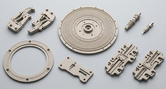
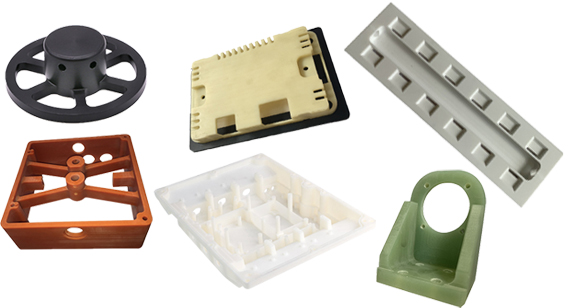
With its stable electrostatic dissipative performance under strong electric fields, high mechanical rigidity, and excellent heat resistance, Semitron ESd 520HR is widely used in semiconductor front-end processes, back-end testing, and other industries with stringent requirements for static electricity, vacuum, and high temperatures, such as:
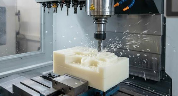
Precision tolerances (±0.02 mm) for Semitron 520 (PAI) can only be achieved through CNC machining; other processes, such as injection molding or 3D printing, cannot meet these tolerance requirements. However, it is important to note that selecting CNC machining to produce Semitron 520 precision electronic or semiconductor parts requires considering manufacturing limitations such as warping, thin-wall control, and dimensional stability, which imposes certain requirements on your part drawing design. These considerations are discussed by case below:
1. Warping Prevention and Deformation Control
The base resin (PAI) of Semitron 520 possesses high internal residual stress. Although the factory utilizes processes like separating rough and finish machining, stress-relief annealing, and symmetrical cutting to significantly reduce the risk of bending and warping deformation during or after machining, the part design must still remain within a reasonable range.
Drawing Design Requirements:
2. Thin-Wall Structure Design Limitations
While Semitron 520 possesses extremely high mechanical rigidity, it also exhibits a certain degree of brittleness—designs exceeding thin-wall limit requirements easily lead to high rejection rates. Although CNC machining can ensure machining stability by selecting high-speed, high-sharpness specialized plastic milling cutters and adjusting the sequence (machining thin-walled areas last), the part design must still maintain a reasonable dimensional range to prevent micro-chatter during cutting from affecting the achievement of the 0.02 mm tolerance.
Drawing Design Requirements:
3. Preventing Stress Concentration Caused by Unreasonable Geometric Design
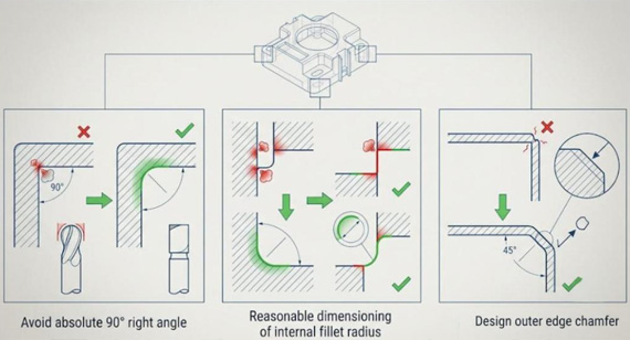
Semitron 520 is relatively sensitive to stress concentration. Inappropriate geometric part designs will cause stress concentration, affecting machining and subsequent service life.
Drawing Design Requirements:
4. Moisture Absorption Dimensional Tolerance Compensation
The Semitron 520 PAI base material has strong moisture absorption characteristics. On the manufacturing side, tolerances can be controlled through a series of strict procedures, such as rapid machining in a constant temperature and humidity workshop, immediate sealed and dry storage after machining, and low-temperature baking before service. However, regarding the operating environment, you need to consider how moisture absorption characteristics affect application tolerances:
Precision Tolerance Labeling: For pinholes or axial dimensions requiring micron-level precision fits, it is recommended to reserve a moisture absorption expansion allowance of 0.03% - 0.05% in advance when labeling drawing tolerances, or note on the drawing: "Tolerance dimensions should be measured when the material is completely dry (moisture content < 0.1%)."
5. Reducing Heat Accumulation
The thermal conductivity of Semitron 520 is low, and frictional heat during the machining process easily accumulates in the cutting zone (causing inaccuracies and surface roughness). The machining end will dissipate heat by selecting carbide/PCD tools, adopting a "fast-in, fast-out" cutting strategy, and spraying sufficient water-soluble coolant; meanwhile, a reasonable drawing design can also reduce heat accumulation:
Drawing Design Requirements:
Is Semitron 520 An Expensive Material?
Yes, it is relatively expensive. As a specialty engineering plastic modified from a polyamide-imide (PAI) base resin, Semitron 520 belongs to the high-end electrostatic dissipative (ESD) material category. Due to its complex synthesis process, the procurement unit price for a single sheet or rod is higher than that of ordinary anti-static POM or PEI. Excluding cross-border logistics and other fees, you can refer to the following approximate market prices (prices fluctuate and are for reference only):
Is The Cnc Machining Cost Of Semitron 520 High?
It is relatively high, but its cost matches its high-value-added operating conditions. The high machining cost is primarily due to:
Since Cnc Machining Uses a Subtractive Process, Doesn't It Cause Semitron 520 Material Waste And High Costs?
Although it is a subtractive cutting process, this cost expenditure is necessary when dealing with a 0.02 mm accuracy requirement, especially for semiconductor industry applications.
Process Irreplaceability:
Although injection molding (near-net-shape forming) and 3D printing (additive) processes have obvious advantages in material utilization, these processes still have limitations when facing precision parts like semiconductor test fixtures and wafer grippers that require 0.02 mm-level geometric tolerances, ultra-high flatness, and low internal stress.
Injection-molded parts are prone to anisotropy caused by uneven cooling, warping deformation, and post-shrinkage rates, making it very difficult to stably meet technical indicators.
3D printing is limited by layering resolution, surface roughness (Ra), and microscopic anisotropy caused by interlaminar bonding forces. When directly forming high-performance PAI (such as Semitron 520), it is difficult to guarantee the circularity and density of precision hole positions, posing a high risk of outgassing in high-vacuum environments.
Cost Control:
Furthermore, although machining chips are difficult to recycle and reuse at equal value due to material properties, experienced CNC machining factory usually controls material costs through the following methods:
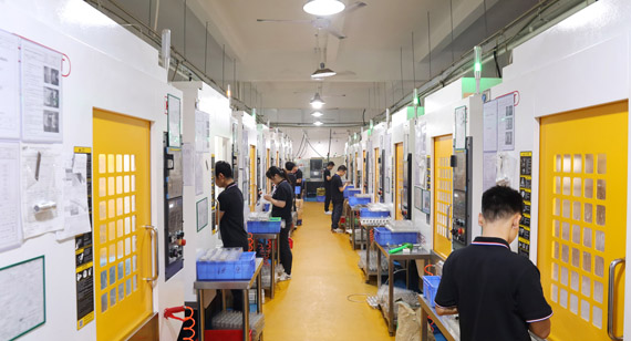
A well-known client in the European semiconductor industry approached us to machine a high-speed suction nozzle holder assembly used in back-end testing handlers. The part design required no dielectric breakdown under extreme high temperatures and high-frequency strong electric field conditions, so the specified material was Semitron ESd 520HR (PAI), and the tolerance of the displacement mating hole was strictly controlled within plus or minus 0.02 mm. Because the client's previous supplier failed to well balance the high internal stress and strong moisture absorption of the PAI material, the yield rate of the finished products was low, and the parts suffered from microscopic cracking and out-of-tolerance issues.
Upon receiving this project, our engineering team took the following measures:
Results: The first-article inspection yield rate for this batch of precision components reached as high as 98.5%. The pinholes not only met the plus or minus 0.02 mm tolerance, but the edges of the micro-holes also showed zero microscopic cracks under an electron microscope. After being cleaned with alcohol and dried at a low temperature to remove water, the parts were immediately packed and sealed in moisture-proof vacuum bags containing industrial desiccants for delivery. Once put online, the product demonstrated excellent dimensional stability and service life on the client's semiconductor testing line.
As an electrostatic dissipative specialty engineering plastic, Semitron ESd 520HR (PAI) has become a choice material for semiconductor front-end wafer manufacturing, back-end precision test fixtures, aerospace, medical, and precision electronics, thanks to its unique property of experiencing no dielectric breakdown under continuous high-voltage strong electric fields, as well as its excellent heat resistance and dimensional stability. However, the flip side of high performance is its strict requirements on the machining and design sides. To stably achieve a precision tolerance of 0.02 mm, the geometric structural design of the part and the scientific labeling of dimensional tolerances must be deeply coordinated with the CNC machining end processes (such as step-by-step cutting, stress-relief annealing, and moisture control). Although the material itself and the subtractive machining costs are relatively expensive, the long-term service benefits it brings are well worth the initial investment in industries like semiconductor and high-end electronics manufacturing, which demand high yield rates and reliability.
Have you also encountered similar issues with Semitron 520 parts regarding deformation control or micro-hole edge chipping? Welcome to contact our engineering team to get a free consultation, or send your drawings to us for a free DFM design evaluation and CNC machining quote. [2D Drawings (PDF files), 3D Drawings (IGS/STP/STEP files)]

Q1: What are the advantages of Semitron 520?
Its core advantage is its extremely stable electrostatic dissipative performance under strong electric fields, combined with excellent mechanical rigidity, wear resistance, and a continuous heat resistance capacity of 260°C.
Q2: What are the disadvantages of Semitron 520?
The main disadvantage is its significant tendency to absorb water, which can easily cause minor dimensional drift in humid environments. Additionally, it is sensitive to chemical environments and is not resistant to acids and bases.
Q3: Can Semitron 520 use injection molding or 3D printing to reduce costs?
Theoretically, material waste can be reduced through additive or near-net-shape molding; however, for applications like semiconductor testing that demand a precision tolerance of 0.02 mm, CNC subtractive machining remains the only option to ensure accuracy and yield rates.
Q4: Why is it not recommended to design absolute 90° right angles for Semitron 520 on part drawings?
Because the material exhibits a certain degree of brittleness and is highly sensitive to stress concentration, absolute 90° right angles are prone to edge chipping or cracking due to instantaneous impact or concentrated stress during CNC corner clearing or while under stress in service.
Q5: How should Semitron 520 precision parts be stored?
They should be sealed in moisture-proof bags containing desiccants and stored in a warehouse with constant temperature and humidity.
Q6: What preparation is required when using Semitron 520 parts in high-temperature environments?
Before entering high-temperature (260°C) service, the parts need to undergo low-temperature stepped dehydration drying in an oven at 120°C to 150°C to prevent trace moisture absorbed inside from vaporizing at high temperatures, which could cause surface blistering or delamination.
The technical information and manufacturing advice shared on the VMT website are for general guidance only. While we strive for accuracy, VMT does not guarantee that the processes, tolerances, or material properties mentioned are applicable to every specific project. Any reliance you place on such information is strictly at your own risk. It is the buyer's responsibility to provide definitive engineering specifications for any production orders. Final specifications and service terms shall be subject to the formal contract or quotation confirmed by both parties.


 +86 15099911516




 Read more